
Atomic Force Microscopy study of hexagonal boron nitride film growth on 6H-SiC (0001)
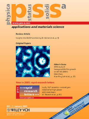 Boron nitride thin films with their
unique mechanical and electrical properties are of interest for
various applications and have been grown on a number of different
substrates. The cover picture from this issue's Editor's Choice [1]
shows an Atomic Force Microscopy topography of a hexagonal BN film
grown on 6H-SiC substrate by Plasma Enhanced Chemical Vapor
Deposition at 600 °C. Interesting stress-relief features developed
on the non-reactive substrate. The corresponding author Kian Ping
Loh is Assistant Professor at the National University of Singapore.
His research is devoted to the growth of diamond and boron nitride
thin films and the fabrication of nanocrystalline diamond and boron
nitride nanotubes.
Boron nitride thin films with their
unique mechanical and electrical properties are of interest for
various applications and have been grown on a number of different
substrates. The cover picture from this issue's Editor's Choice [1]
shows an Atomic Force Microscopy topography of a hexagonal BN film
grown on 6H-SiC substrate by Plasma Enhanced Chemical Vapor
Deposition at 600 °C. Interesting stress-relief features developed
on the non-reactive substrate. The corresponding author Kian Ping
Loh is Assistant Professor at the National University of Singapore.
His research is devoted to the growth of diamond and boron nitride
thin films and the fabrication of nanocrystalline diamond and boron
nitride nanotubes.
As a follow-up to the recent special issue on Physics of Organic Semiconductors [2], Detlef Berner gives insights into organic light emitting diode functioning by coordinated experiment and simulation in his Review Article [3].
The present issue also sees the start of our rapid research letters, the fastest peer-reviewed publication medium in solid state physics. For more information see www.pss-rapid.com and the Editorial by the Editor-in-Chief Martin Stutzmann on page 7 [4].