| RESEARCH |
Our research can be broadly classified into:
Our Signature research programmes includes:
-
Organic UltraDoping Technology
-
Polymer Semicond Crosslinker Technology
-
Graphene-Hybrid Technology
-
Nanometal Ink Technology
-
Plastic Thermoelectric Generator Film Technology
-
Inkjet Printing Knowhow
|
| Device Chemistry |
The device chemistry thrust conducts research in the following key areas:
Structure−morphology − property relations
Good device performance, whether in organic light-emitting diodes, transistors or solar cells, depends not only on the chemical structure of the materials but also on their morphology in the solid film. We have therefore placed significant emphasis on the study of the structure−morphology−property relations of polymer and oligomer semiconductors and of solution-prccessable graphenes.
We typically employ a variety of techniques, including atomic force microscopy, scanning electron microscopy, variable-temperature (VT) X-ray diffraction, VT-UV-Vis-infrared spectroscopy, VT Raman spectroscopy, VT variable-angle spectroscopic ellipsometry, polarising optical microscopy, ultraviolet photoemission spectroscopy, together with variable-temperature device characterisations, to determine these relations.
|
|
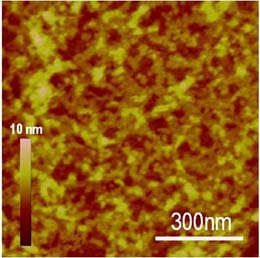
Terrace-morphology induced for the first time in P3HT films, giving at least one order of magnitude improvement in their field-effect mobility.
|
Device degradation mechanisms
Device degradation is an extremely important topic in the technology of plastics electronics. However their underlying mechanisms have been rarely investigated in the literature. Here we have a programme of research to study the intrinsic degradation mechanisms of the pi-conjugated semiconductors during device operation.
We have discovered the following mechanisms so far: (i) injection-dedoping of p-doped conducting polymer film in light-emitting diodes, (ii) electromigration of doped conducting polymer chains in the polymer film, and (iii) photoinduced doping of transistor semiconductor films promoted by oxygen/moisture. Elucidation of the fundamental mechanisms will reveal new strategies for improving the storage and operational lifetimes of plastic electronic devices. We work on some of these topics with our industrial partners.
|
|
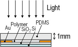
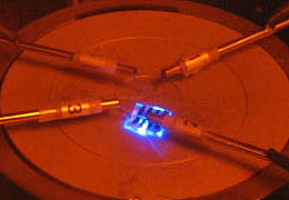
Field-effect transistor device under light illumination
|
Materials development
We have a materials development programme to synthesise novel advanced functional materials for specific applications. This includes inkjet-printable functional inks, photocrosslinkers, solar-cell materials, and solution-processable graphenes. This materials development programme complements those of our collaborators both in the industry and academia.
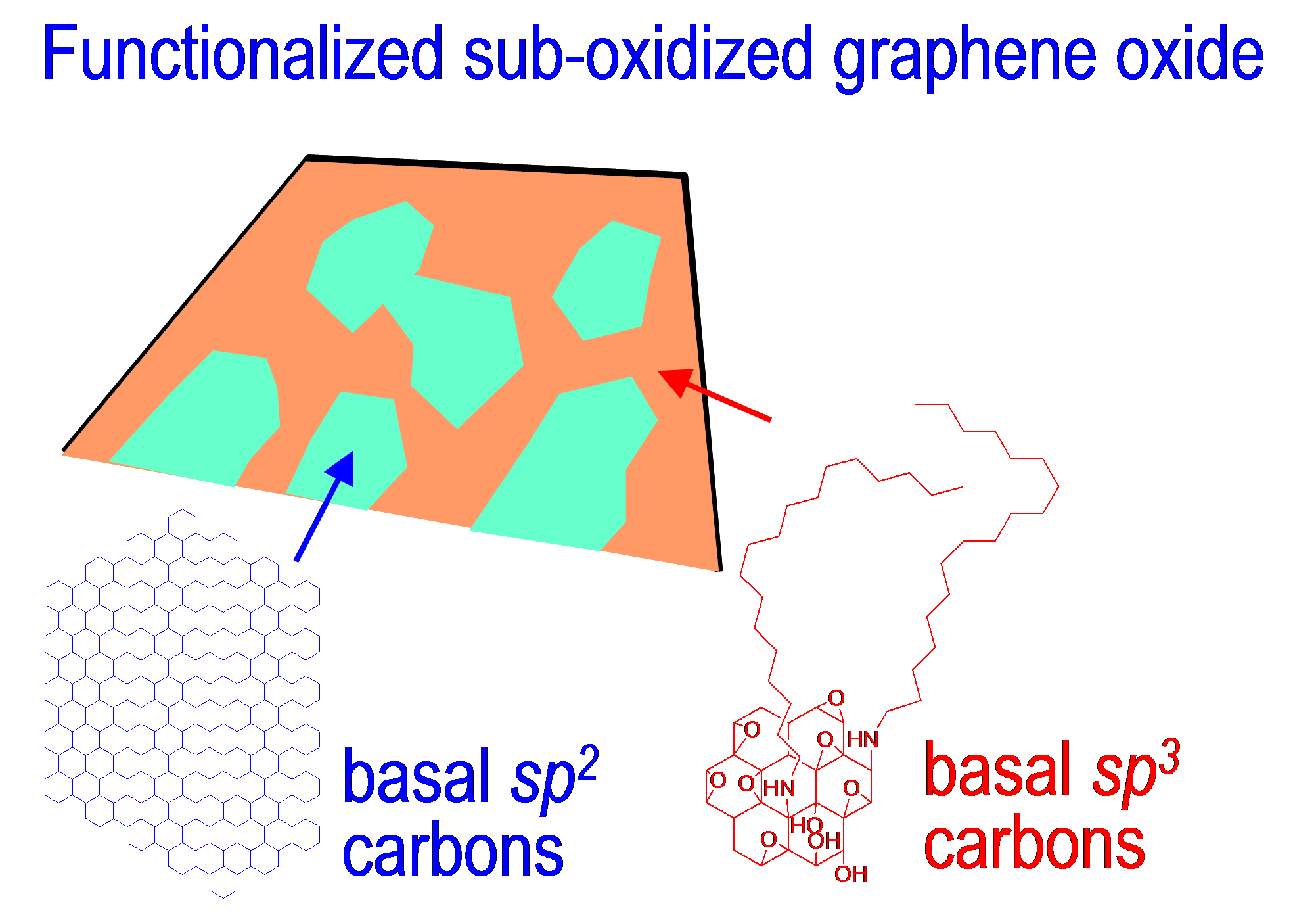
For example, we have successfully developed low-sintering-temperature nanometal inks that are compatible with plastic electronics; general-purpose photocrosslinker additives that can be formulated into a wide of polymer semiconductors to make quality heterostructures for high-performance devices; synthesis of functionalized sub-oxidized graphene oxide that are highly-dispersible in organic solvent, hence they can be blended into polymer solutions and formed thin or thick nano-composite films using general solution-processing technique such as printing, spin-coating and spraying.
This programme of research is strongly supported by in-house characterisation and device fabrication capabilities.
|
|
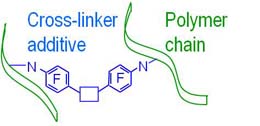
We develop cross-linker additives that can be formulated into semiconductor polymer films to give crosslinked polymers suitable for the production of organic semiconductor heterostructures.
|
|
We have synthesized functionalized sub-oxidized graphene oxide sheets that are dispersible in organic solvents and can be sprayed-coated to form film on plastic PCB substrates.
|
|
Video:spray-coating
|
|
The device physics thrust conducts research in the following key area:
Science and technology of Ohmic contacts
Development of Ohmic contacts in which the injected current is not limited by interface resistance is a central goal of the device engineering of metal/ organic semiconductor contacts. However the physics underpinning the correct description of the energy-level alignment at such contacts appears to still be incomplete.
We have therefore placed significant emphasis on the study of the interface carrier energetics in devices. Our main techniques are: (i) home-built electromodulated absorption (EA) spectroscopy to extract both the diode built-in potential and sub-gap polaron absorption, (ii) home-built internal photoemission spectroscopy to extract the carrier injection barrier, supported by (iii) conventional ultraviolet photoemission spectroscopy of energy-level alignment. We have also been extensively mapping out the behaviour of doped interfaces.
The aim is to develop general Ohmic hole and electron contacts, which are important in organic light-emitting diodes, transistors, and solar cells.
|
|
Development of Ohmic contacts is not only important in high-performance organic light-emitting diodes (pictured), but also in field-effect transistors and solar cells.
|
The nature of charge carriers in organic semiconductors
There is exciting recent research from our group (and others) suggesting that charge-carriers can be in fact be delocalised between chains in polymer organic semiconductors. This is a prerequisite for true band transport of carriers in polymer semiconductor films.
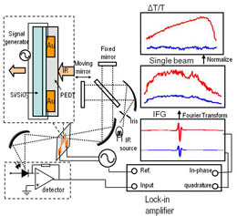
We have therefore been investigating the nature of charge carriers particularly in field-effect transistors (FETs). Our main technique is charge-modulation spectroscopy (CMS). We have developed a CMS technique spanning the UV-Vis-NIR-IR spectral regions. In particular our IR-CMS technique is based on a new method of interferogram modulation developed in-house which gives an unprecedented signal-to-noise ratio and both in-phase and quadrature information that are not available elsewhere.
The aim is to achieve new understanding of the nature of charge carriers in devices, what limits their macroscopic mobility, and how they interact for example with interfaces, as a key step to developing higher performance materials and devices.
|
|
CMS is an electro-optical spectroscopic technique that allows the properties of charge carriers present in the conduction channels of FETs and other device structures to be studied in situ. This allows direct observation of the charge carriers in the device via their spectroscopic signatures. |
Physics of organic solar cells and transistors
We have a research programme to study the physics in particular of polymer organic solar cells and transistors. This is an experimental effort heavily supported by computational modeling, e.g., modeling of the exciton-generation profile within the devices using transfer matrix methods, and fitting of the entire mobility−temperature−carrier density surface to density-of-states models.
We have to date for example fully mapped out the power-conversion efficiency landscape for the conventional regioregular poly(3-hexylthiophene): phenyl-C61-butyric acid methyl ester light-harvesting system.
The aim is to achieve new understanding in the physics of organic semiconductor devices to provide a proper basis for their optimisation.
|
|
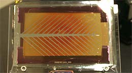
A 4x6-in organic solar cell made by ONDL for the 80th Anniversary of the Faculty of Science NUS celebrations/ exhibition. This cell is able to run four toy cars simultaneously under the sun. |
|
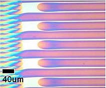
The device processing thrust conducts research in the following key area:
Development of IJP methodology and protocol
Inkjet printing as a deposition produces a fundamentally different polymer film morphology (i.e., packing, interchain order, and crystallinity) than spin-cast or doctor-blade films. Furthermore the printed film morphology depends strongly on confinement of the liquid droplet or film.
We have therefore developed a programme of research to investigate (i) inkjet-printed film morphology and its correlation with device performance (field-effect transistors and solar cells), (ii) jettability of inks, i.e., whether the ink can be ejected by the printhead, and printability of substrate, i.e., whether the desired printed shape can be achieved, and (iii) use of surface energy patterns to control the confinement of the printed droplets and films.
The aim of this programme is to develop in-house printing protocols in support of industrial partners.
|
|
We investigate printing methodologies for plastic electronics.
|
| |
Some of our projects are funded by: |
| |
|
 |
 |
|
 |
 |
|
|
 |
| |